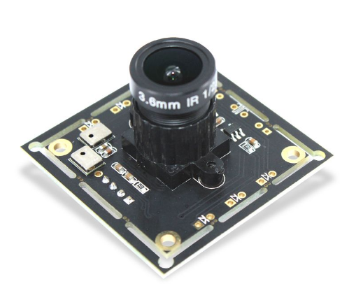
A Complete Guide to Understanding Camera Module PCB
The Camera Module PCB (Printed Circuit Board) is a critical component in modern digital cameras, smartphones, surveillance cameras, and many other imaging devices. It serves as the backbone that connects and controls the various electronic components responsible for capturing, processing, and transmitting images and videos. In this comprehensive guide, we'll delve into the key aspects of Camera Module PCBs, explaining their structure, functionality, and importance in the world of imaging technology.
1. Introduction to Camera Module PCBs:
A Camera Module PCB is a specialized circuit board designed to support the operation of a camera's imaging sensor, lens assembly, image processing units, and various other components. It acts as an interface between these elements, facilitating the transfer of data, control signals, and power, while also ensuring the mechanical stability of the camera module.
2. Components of a Camera Module PCB:
A typical Camera Module PCB comprises several essential components:
- Image Sensor: This is the core component that captures light and converts it into electrical signals. There are various types of image sensors, including CMOS (Complementary Metal-Oxide-Semiconductor) and CCD (Charge-Coupled Device).
- Lens Assembly: The lens assembly includes one or more lenses that focus light onto the image sensor. Some camera modules have fixed lenses, while others feature interchangeable lenses for greater versatility.
- Control ICs (Integrated Circuits): Control ICs manage the operation of the image sensor, control the lens focus and zoom, process image data, and handle communication with other device components.
- Connectors: These are used to establish connections between the Camera Module PCB and the main PCB of the device (e.g., a smartphone or digital camera). Connectors may include FPC (Flexible Printed Circuit) connectors or soldered connections.
- Flexible Printed Circuit (FPC) or Ribbon Cables: FPCs are thin, flexible cables that transmit electrical signals and data between components. They are often used to connect the image sensor to the PCB and other elements.
- Passive Components: These include resistors, capacitors, and inductors that help regulate electrical signals, filter noise, and stabilize the power supply.
- Power Management Components: Voltage regulators and power management ICs ensure that the camera module receives stable and appropriate power levels for its operation.
- Shields and EMI (Electromagnetic Interference) Protection: Shielding components and EMI protection measures are employed to reduce interference and maintain signal integrity.
HBVCAM OV9732 1MP 720P HD USB Camera Module with OTG function
3. Functions of a Camera Module PCB:
The Camera Module PCB plays several crucial roles in the overall functionality of a camera module:
- Signal Processing: The PCB processes the electrical signals generated by the image sensor, adjusting factors like exposure, white balance, and color correction to produce high-quality images.
- Data Transfer: It facilitates the transfer of image and video data from the image sensor to the main processing unit of the device, allowing for real-time preview and storage.
- Control: The PCB manages various aspects of the camera's operation, including focus control, zoom, aperture adjustment, and image stabilization.
- Power Distribution: It ensures that the camera module receives the appropriate voltage levels to operate efficiently while also managing power consumption to extend battery life in portable devices.
- Communication: In devices with multiple cameras, the Camera Module PCB may manage the synchronization and switching between camera modules.
4. Design Considerations for Camera Module PCBs:
Designing a Camera Module PCB involves several critical considerations:
- Size and Form Factor: The PCB must fit within the confines of the camera module's housing. Miniaturization is often a crucial factor in modern device design.
- Signal Integrity: Maintaining signal integrity is essential for high-quality image capture. The PCB design should minimize electromagnetic interference and signal loss.
- Power Efficiency: Efficient power management is vital for battery-powered devices, ensuring that the camera module operates without draining the battery too quickly.
- Thermal Management: As cameras can generate heat during extended use, effective thermal management is essential to prevent overheating, which can degrade image quality or damage components.
- Reliability and Durability: Camera modules may be subjected to various environmental conditions, including temperature variations, humidity, and mechanical shocks. The PCB design should account for these factors to ensure long-term reliability.
- Cost Optimization: Designing cost-effective PCBs without compromising performance is crucial for mass production and market competitiveness.
5. Challenges and Advances:
The development of Camera Module PCBs is an ongoing process, driven by technological advancements and the demand for higher image quality and functionality. Some of the challenges and recent advances in this field include:
- Miniaturization: Advances in PCB manufacturing have enabled the development of smaller and thinner camera modules for compact devices.
- Multi-Camera Integration: The integration of multiple camera modules with varying focal lengths and capabilities has become common, requiring sophisticated PCB designs to manage switching and synchronization.
- High-Resolution Imaging: As consumers demand higher resolution images and 4K or even 8K video recording, PCBs must support the increased data processing and transmission demands.
- AI and Computational Photography: PCBs now often incorporate AI (Artificial Intelligence) processors for features like scene recognition, image enhancement, and computational photography.
- 3D Sensing: For applications like facial recognition and depth sensing, camera modules with specialized sensors are becoming more prevalent, requiring innovative PCB designs.
Conclusion:
Camera Module PCBs are integral to the operation of modern imaging devices, from smartphones to digital cameras and beyond. Understanding their functions and design considerations is essential for anyone interested in the world of photography, imaging technology, or electronics. As technology continues to advance, Camera Module PCBs will play an increasingly critical role in shaping the future of imaging devices and the way we capture and interact with the world around us.

评论
发表评论